Vias, they are very important design elements for all double sided and multi-layers PCB.
They are the plated holes which used to connect 2 layers together, but no components soldering through it. It can join traces, pads and other conductive elements on PCB through a copper placed inside holes.
PCB vias need a certain volume of copper on a layer to ensure that the layers are really connected. So the via ring or PAD, it is a circle of copper, and is connected to the endpoint of traces, specifically narrow ones.
3 Kinds of Vias
So far we know what is via. Let’s get know what kinds of vias we have in design usually.
A. Through Vias
B. Blind Vias
C. Buried Vias
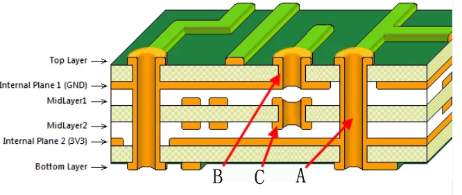
Through Vias, means the via pass through the whole board, from the bottom side to the top side. It is widely existed on all of the double or multilayers PCB.
Blind Vias, means the via connects an outer (visible)layer to an inner(invisible) layer.
Buried Vias, means the via connects inner layer to inner layer. It is invisible.
Naturally, blind vias and buried are only designed on multilayers PCB, and the costs is much higher. Buried vias are barely used unless nescessary because they are harder to troubleshoot.
Methods of vias treatment
Usually there are 3 kinds of way to finish the via:
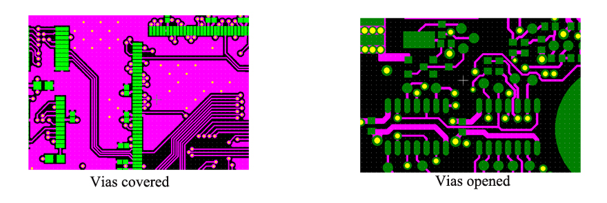
1. Vias covered/tented
2. Vias filled/pluged
3. Vias opened
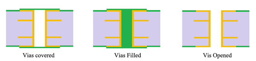
Those are 3 kinds of finishing for the vias with normal costs.
First, for all of vias, they have copper plated through the hole wall, copper is used to connected different layers trace or pads, and then fulfill it’s function. And then covered the surface of vias by solder mask, that is called vias covered or tented. You can still see the light through the hole.
If we fill the whole via with solder mask, you can not see the light through the hole, then that is the way for vias filled/pluged.
And for vias opened, that means to open the via with no solder mask, covered it with the same material as other soldering PADs. If the PCB finishing is HASL, then then via will have a HASL Ring, and also HASL through the hole.
If the PCB finishing is Immersion Gold, the vias will be covered by gold, including the wall of the vias. It is just like other soldering holes, you can see other side through the holes.
Some rules of vias you need to follow during designs
1. Do not design the vias on the PADs.
2. No vias in the patch glue dispensing or printing area. For example, the PCB area under the CHIP and SOP components using chip glue dispensing or printing process
3. No vias in the area where the metal shell of the device and the PCB contact area extends 1.5mm.
4. Usually, it is better to design the diameter of the vias bigger than 0.2 mm(8 mil). 0.3 MM vias can get the normal price. 0.2 mm price higher than 0.25 mm, and 0.25 mm size higher than 0.3 mm.
For 0.15 mm Vias, the costs is much higher. Many company can not make it.
But it is not a problem for crown key pcb.
For 0.1 mm Vias, it needs to use laser drill. Send us the design file, our engineer will calculate the costs.
5. It is not recommended to use buried and blind vias for 0.65 mm or bigger BGA. The costs will be increased significantly.
6. The distance between vias should not be too close. It is easy to break the holes if they are too close. Usually the distance needs to be 0.5 mm or bigger. 0.35mm-0.4mm distance should be avoided, and 0.3mm or smaller are prohibited.
Some customer would ask, how to manufacture the vias as we want?
Here are the answers:
1. If you want the vias covered or filled, do not design PADs on solder mask layer.
And you have to tell the engineer that you want them just covered, or you need them filled.
2. If you want the vias opened, then you need to design PADs on solder mask layer.
If any doubt about vias, please contact our email: jack@crown-key.com; Our team will be very glad to share with you more details.